The Tech Revolution of "Teflon": The Invisible Guardian Behind Semiconductors
In the realm of chip manufacturing, which can be called the pinnacle of human industrial precision, everything is bathed in pure white light. Engineers clad in cleanroom suits operate multi-million-dollar equipment with the precision of surgeons. Yet, few realize that in this world of silicon and nanoscale competition, a seemingly ordinary plastic—polytetrafluoroethylene (PTFE), known commercially in everyday life as the non-stick coating "Teflon"—plays an indispensable role as an "invisible guardian."
I. The "Ultimate Fastidiousness" of Semiconductor Manufacturing and the Ultimate Test for Materials
Chips, especially high-end processors, are made by integrating tens of billions of transistors onto a silicon wafer the size of a fingernail through thousands of process steps. Any minuscule contamination—be it a speck of dust or a single metal ion—can lead to the scrapping of an entire batch of chips, resulting in losses of millions of dollars. Therefore, semiconductor fabs impose (near-fanatical) demands on the cleanliness, stability, and purity of all materials used.
This presents three ultimate tests for any material used in the manufacturing process:
Ultra-Pure and Non-Contaminating: The material itself must not leach any ions or particles that could pollute the process environment.
Extreme Corrosion Resistance: It must withstand repeated assaults from the most aggressive acids, alkalis, strong oxidizers, and high-temperature plasmas.
Absolute Performance Stability: Under severe temperature fluctuations and high vacuum environments, it must not deform, volatilize, or suffer performance degradation.
Specially treated fluoropolymer materials happen to be the "all-rounders" that can perfectly pass these tests.
II. Why Are Fluoropolymer Materials the "Chosen Ones"?
Fluoropolymer materials, especially Polytetrafluoroethylene (PTFE), Perfluoroalkoxy (PFA), and Perfluoroelastomer (FFKM), possess a series of astounding innate qualities:
Absolute Inertness of the "Plastic King": Its molecular structure is exceptionally stable, reacting with almost no known chemical substances. Whether it's aqua regia, hydrofluoric acid, or concentrated sulfuric acid, they all pale in its presence.
"Slippery Non-Stick" Surface: Its extremely low surface energy grants it (exceptional non-stick properties). Various chemical liquids and particles find it hard to adhere and are easily washed away, reducing contamination sources at the root.
High-Purity Potential: Through special purification processes, it can achieve "electronic grade" ultra-high purity. The leachate of metal ions can be controlled at parts per billion (ppb) levels, perfectly meeting the semiconductor industry's (stringent) purity requirements.
Broad Temperature Adaptability: It can withstand short-term high-temperature processes exceeding 250°C while remaining flexible and not brittle at cryogenic temperatures as low as -100°C.
These properties make fluoropolymer materials the ideal gear for traversing the "perilous path" of semiconductor manufacturing.
III. Ubiquitous Protection: A Tour of Fluoropolymer Product Applications in a Chip Fab
Walking into a chip production line, you'll find fluoropolymer products everywhere:
"Loyal Vessels" for Wet Processes: In cleaning and etching steps, storage tanks, pipes, valves, and pump bodies holding various ultra-high purity chemicals are mostly made of PFA or PTFE. They ensure the chemicals remain (extremely pure) upon reaching the wafer surface, uncontaminated by the vessels themselves.
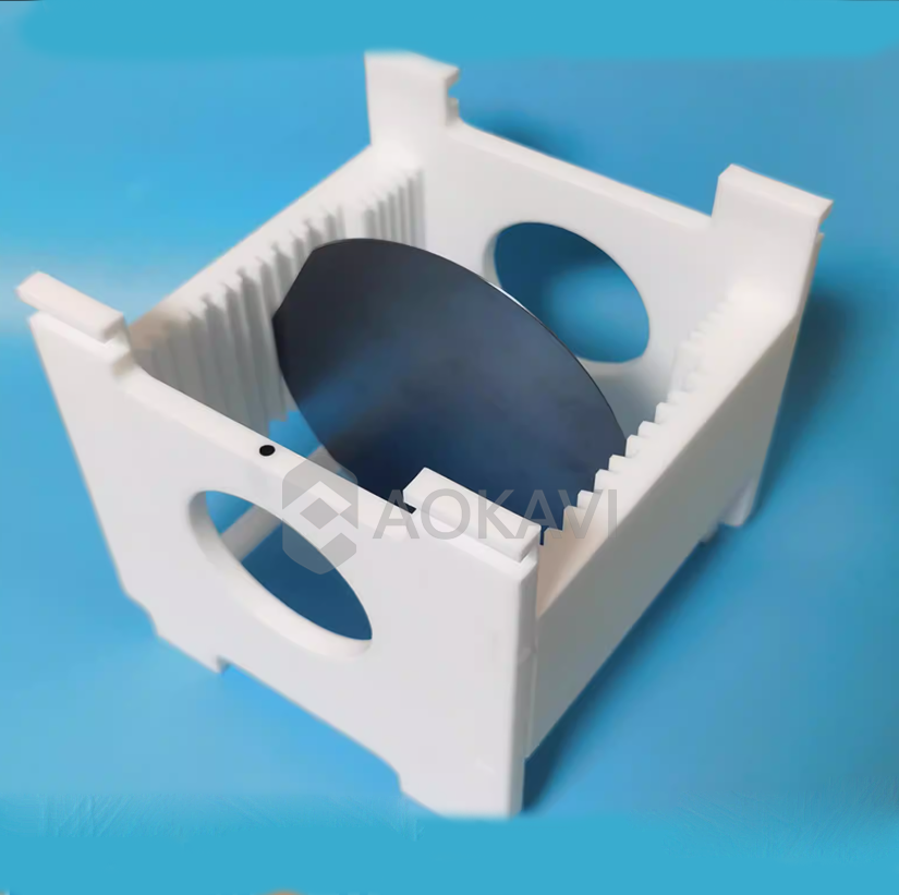
The "Perfect Chassis" for Wafers: During transportation and processing, wafers need to be carried. Wafer carriers (Cassettes) and boats made from PFA can safely support these invaluable "glass disks," shuttling them between various reaction chambers, thanks to their dust-free, metal-free, and corrosion-resistant properties.
"Precision Vasculature" for Special Gas Systems: Chip manufacturing requires the use of highly toxic and corrosive special gases like silane and phosphine. The inner walls of piping systems delivering these "beasts" must be lined with PTFE or PFA, ensuring the gases do not react or become contaminated during long-distance transport, ultimately participating in reactions precisely.
"Sturdy Armor" Against Plasma: In etching and deposition steps, high-temperature plasma is generated, which is extremely corrosive. Internal components of the reaction chamber, such as focus rings, insulation parts, and seals, are largely made from PTFE or FFKM materials, known for their (strong plasma corrosion resistance), protecting the core components of expensive equipment.
"Pure Conduits" for Ultrapure Water: The ultrapure water used to rinse chips is far purer than drinking water. Pipes, valves, and filter housings in its distribution system are also commonly lined with fluoropolymer materials, ensuring the "final rinse" is not (re-contaminated) by the pipes themselves.
Conclusion: The Foundational Power of Unsung Heroes
When we marvel at the powerful computing capabilities of a new generation of chips, we should not forget that behind this brilliance lies breakthroughs and support from countless fundamental material sciences. Fluoropolymer products are like the unsung crew members behind the stage. They don't perform directly but build the safest and purest stage, ensuring the "lead actor," the silicon wafer, performs perfectly. This glamorous transformation of "Teflon," from pots and pans to critical national instruments, is a classic example of material science deeply empowering modern high-tech industries. It tells us that true technological revolution often stems from these seemingly ordinary yet vital invisible foundations.